68
9151AINDCO07/09
ATA8742
18. External Interrupts
The External Interrupts are triggered by the INT0 pin or any of the PCINT11..0 pins. Observe
that, if enabled, the interrupts will trigger even if the INT0 or PCINT11..0 pins are configured as
outputs. This feature provides a way of generating a software interrupt. Pin change 0 interrupts
PCI0 will trigger if any enabled PCINT7..0 pin toggles. Pin change 1 interrupts PCI1 will trigger if
any enabled PCINT11..8 pin toggles. The PCMSK0 and PCMSK1 Registers control which pins
contribute to the pin change interrupts. Pin change interrupts on PCINT11..0 are detected asyn-
chronously. This implies that these interrupts can be used for waking the part also from sleep
modes other than Idle mode.
The INT0 interrupts can be triggered by a falling or rising edge or a low level. This is set up as
indicated in the specification for the MCU Control Register MCUCR. When the INT0 interrupt is
enabled and is configured as level triggered, the interrupt will trigger as long as the pin is held
low. Note that recognition of falling or rising edge interrupts on INT0 requires the presence of an
I/O clock, described in
Clock Systems and their Distribution
on page 41. Low level interrupt on
INT0 is detected asynchronously. This implies that this interrupt can be used for waking the part
also from sleep modes other than Idle mode. The I/O clock is halted in all sleep modes except
Idle mode.
Note that if a level triggered interrupt is used for wake-up from Power-down, the required level
must be held long enough for the MCU to complete the wake-up to trigger the level interrupt. If
the level disappears before the end of the Start-up Time, the MCU will still wake up, but no inter-
rupt will be generated. The start-up time is defined by the SUT and CKSEL Fuses as described
in
System Clock and Clock Options
on page 41.
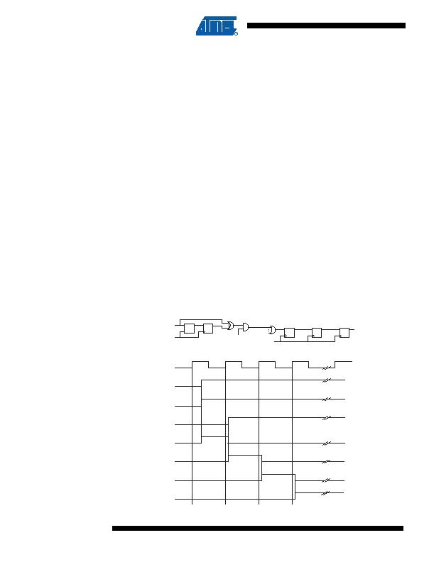
18.1 Pin Change Interrupt Timing
An example of timing of a pin change interrupt is shown in Figure .
Timing of pin change interrupts
clk
PCINT(0)
pin_lat
pin_sync
pcint_in_(0)
pcint_syn
pcint_setflag
PCIF
PCINT(0)
pin_sync
pcint_syn
pin_lat
D Q
LE
pcint_setflag
PCIF
clk
clk
PCINT(0) in PCMSK(x)
pcint_in_(0)
0
x
发布紧急采购,3分钟左右您将得到回复。
相关PDF资料
ATA8743-PXQW
MCU W/TRANSMITTER ASK/FSK 24QFN
ATAVRRZ200
KIT DEMO AT86RF230
AV101-12LF
ATTENUATOR HIP3 0.70-1GHZ 8-SOIC
AV102-12LF
ATTENUATOR HIP3 1.7-2GHZ 8SOIC
AV113-12LF
ATTENUATOR HIP3 2.1-2.3GHZ 8SOIC
AXUV100G
SENSOR ELECTRON DETECTION
B0205F50200AHF
XFRMR BALUN RF 200-500MHZ 1608
B0310J50100AHF
XFRMR BALUN RF 300-1000MHZ 0805
相关代理商/技术参数
ATA8743
制造商:ATMEL 制造商全称:ATMEL Corporation 功能描述:Microcontroller with UHF ASK/FSK Transmitter
ATA8743C- PXQW
功能描述:8位微控制器 -MCU Embedded uC incl RF Tx for 315 MHz
RoHS:否 制造商:Silicon Labs 核心:8051 处理器系列:C8051F39x 数据总线宽度:8 bit 最大时钟频率:50 MHz 程序存储器大小:16 KB 数据 RAM 大小:1 KB 片上 ADC:Yes 工作电源电压:1.8 V to 3.6 V 工作温度范围:- 40 C to + 105 C 封装 / 箱体:QFN-20 安装风格:SMD/SMT
ATA8743C-PXQW
制造商:Atmel Corporation 功能描述:EMBEDDED ?C INCL RF TX FOR 868 MHZ - Trays 制造商:Atmel Corporation 功能描述:EMBEDDED C INCL 868MHZ TX
ATA8743C-PXQW-1
功能描述:EMBEDDED INCL RF TX FOR 868 MHZ 制造商:microchip technology 系列:- 包装:剪切带(CT) 零件状态:在售 频率:868MHz ~ 928MHz 应用:通用 调制或协议:UHF 数据速率(最大值):32kbps 功率 - 输出:5.5dBm 电流 - 传输:9.8mA 数据接口:SPI 天线连接器:PCB,表面贴装 存储容量:4kB 闪存,256B EEPROM,256B SRAM 特性:- 电压 - 电源:2 V ~ 4 V 工作温度:-40°C ~ 85°C 封装/外壳:24-VQFN 裸露焊盘 标准包装:1
ATA8743-PXQW
功能描述:8位微控制器 -MCU Embedded uC incl RF Tx for 315 MHz
RoHS:否 制造商:Silicon Labs 核心:8051 处理器系列:C8051F39x 数据总线宽度:8 bit 最大时钟频率:50 MHz 程序存储器大小:16 KB 数据 RAM 大小:1 KB 片上 ADC:Yes 工作电源电压:1.8 V to 3.6 V 工作温度范围:- 40 C to + 105 C 封装 / 箱体:QFN-20 安装风格:SMD/SMT
ATAB5275
功能描述:射频开发工具 LF Tx Antenna driver board (TPMS) RoHS:否 制造商:Taiyo Yuden 产品:Wireless Modules 类型:Wireless Audio 工具用于评估:WYSAAVDX7 频率: 工作电源电压:3.4 V to 5.5 V
ATAB5276
功能描述:射频开发工具 1A Antenna Driver Demoboard RoHS:否 制造商:Taiyo Yuden 产品:Wireless Modules 类型:Wireless Audio 工具用于评估:WYSAAVDX7 频率: 工作电源电压:3.4 V to 5.5 V
ATAB5278
功能描述:射频开发工具 LF Tx Antenna driver board (PEG) RoHS:否 制造商:Taiyo Yuden 产品:Wireless Modules 类型:Wireless Audio 工具用于评估:WYSAAVDX7 频率: 工作电源电压:3.4 V to 5.5 V